A-TECH  >  AI - Page Sitemap  >  Производители дизайна макета A-Tech PCB при скидке
Производители дизайна макета A-Tech PCB при скидке

Производители дизайна макета A-Tech PCB при скидке

Толщина
0,4-5,0 мм
Чистота поверхности
Hasl, hal (l.f), ​​Imm Enig / Tin / Silver
Слой
4 слоя
Материал
FR4, FR4 TG150, FR4 TG170
Мин заказа Количество
Нет
Время выполнения продукции
8-20 дней
Поставка потенциала
10000 кв.м.
Сертификация
ISO9001, TS16949, UL, ROHS, REACH.
Условия оплаты
T / T, PayPal, Wu.
Условия отгрузки
EXW, FOB, DDU и т. Д.
Тест
AOI, электрический тест
Стандартный
IPC Class 2, класс 3.
Цена
latest_price
latest_price_title
quantity_needed:
pieces
Электронной почты:

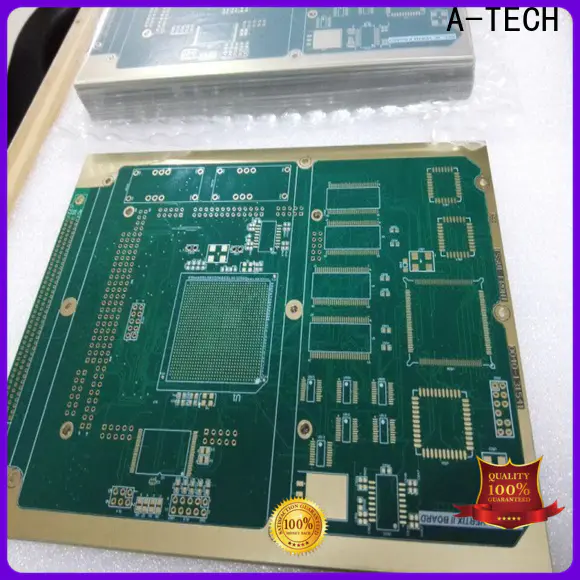
4 Слои PCB - самая большая доля производства печатных плат в A-Tech, у нас огромное преимущество на многослойных печатных платах, потому что у нас есть полный процесс изготовления в доме от внутреннего слоя, ламинирование на разные виды поверхностных отдельных, включают HASL, HAL (LF), ОССП и погружение золота.


The design of A-TECH pcb layout design takes lots of factors into consideration. They include fabric type, coating, tensile strength, and behavior under fire and ultraviolet light. Being laminated by advanced vacuum lamination equipment, it has a uniform dielectric thickness after lamination
The design considerations of A-TECH pcb layout design cover the following aspects: static and dynamic stiffness, operational speeds, gearboxes, manual, and automatic control. Its solderable surface is protected from the oxidation
A-TECH pcb layout design is of professional design. It is based on the knowledge of how manufacturing, surface, and material specifications relate to each other and can affect overall optical performance. Its working panel is coated with a photo-sensitive epoxy-based ink, which can ensure its insulation resistance
The reliability tests for A-TECH pcb layout design is well done. They include temperature&humidity testing, thermal shock testing, leakage current testing, and vibration testing. It has passed AOI which ensures there will be no errors or welding defects
High-quality fabrics are used to make A-TECH pcb layout design with the intention of improving product quality and reducing manufacturing pollution and waste in the industry. Being laminated by advanced vacuum lamination equipment, it has a uniform dielectric thickness after lamination
Its reliability is backed by our expert and experienced professionals. A smooth part is added on its PTH line to reduce the roughness of through hole
Сообщение о продукте
Онлайн чат 编辑模式下无法使用
Онлайн чат inputting
Пожалуйста, держитесь, и мы вернемся к вам в ближайшее время