A-TECH  >  AI - Page Sitemap  >  A-Tech VIA в PAD PCB Hot-Sale для оптовых
A-Tech VIA в PAD PCB Hot-Sale для оптовых

A-Tech VIA в PAD PCB Hot-Sale для оптовых

Min Press Fit Hole
0,5 мм
Толерантность прессы
+/- 2Мил
Мин заказа Количество
Нет
Время выполнения продукции
5-18 рабочих дней
Поставка потенциала
10000 ㎡ / месяц
Сертификация
UL, ISO9001, TS16949
Условия оплаты
T / T, PayPal, WU и т. Д.
Условия отгрузки
EXW, FOB, DDU и т. Д.
Тест
100% электронного теста
Стандартный
IPC класс 2 / класс 3
Цена
latest_price
latest_price_title
quantity_needed:
pieces
Электронной почты:


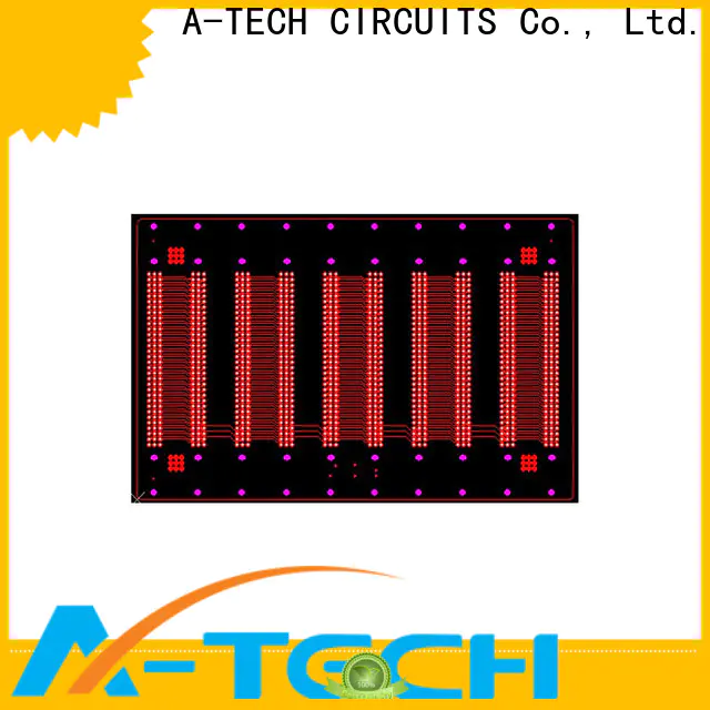
Нажмите PIT HOLE PCB, или нажмите PACB PIND PIND PINS PACB, они компонентные отверстия с медью, покрытым через и с более жестким допуском, чем стандартный PTH, толерантность стандартного ПТГ составляет +/- 0,075 мм (3MIL), но терпимость прессы Отверстие обычно +/- 0,05 мм (2MIL).

Пресс для верхних отверстий используются в качестве отверстий, чтобы соответствовать проводам разъемов, которые не будут припаяны, а нажаты в отверстия. Для того, чтобы приспособиться к свинцам и дыре, чтобы плотно соответствовать, толерантность на обоих хорошо определена, типичные допуски для отверстий для прессы, которые используются при использовании типа, которые используются, и его производитель разъема, который определяет это.

Технология Press Fit Уменьшает время и усилия сборки PCB значительно, и нажмите PIT PIN-код, устраняет необходимость для пайки, это сокращает время и стоимость процесса и повышает производительность производства. Без необходимости припоя модулях инженеры наслаждаются большой гибкостью в дизайне. Модуль может быть легко установлен сверху или снизу PCB без дополнительной стоимости и усилий.

A-Tech Drill Нажмите подходящие отверстия с новыми бурильными битами и управлением специально в процессе изготовления, чтобы обеспечить определенный размер отверстия в толерантности.


A-TECH 2oz copper pcb has to go through a series of manufacturing processes. Its nominal voltage, power source type, water resistance grade, rated power, and insulation have gone through repeated experiments, upgrade, and testing. It is widely used in the chemical industry, metal & mining industry, etc
A-TECH via in pad pcb has been frequently tested by the third-party testing organization. This aims to ensure that it is consistent and compliant with different countries' certifications such as CE, EU, CCC, BEAB, etc. It is extremely popular in Italy, Brazil, Russia, Spain, Australia, and other overseas countries
A-TECH via in pad pcb is a luxury to enjoy every day and night. Using time-honored techniques and crafted of the finest materials, it is manufactured in our own factory in China. The product has low sensitivity to fouling
The package of A-TECH 2oz copper pcb will be done with professional materials. It is packaged with hardened carton, foam, cardboard, or wooden box to protect it in an all-around way to minimize transportation damage. Logo and company nameplate can be made on the product
The timber of log for A-TECH 2oz copper pcb is carefully selected by the QC team. The materials will be tested for water content and harmful formaldehyde content before they are used in production. Supporting low-voltage broadband pulse transmission, it features low consumption
Strict testing: the product undergoes extremely strict testing more than once to achieve its superiority over other products. The testing is conducted by our rigorous testing personnel. Customized catalogs and brochures related to the product are available
Сообщение о продукте
Онлайн чат 编辑模式下无法使用
Онлайн чат inputting
Пожалуйста, держитесь, и мы вернемся к вам в ближайшее время