

Связанные продукты

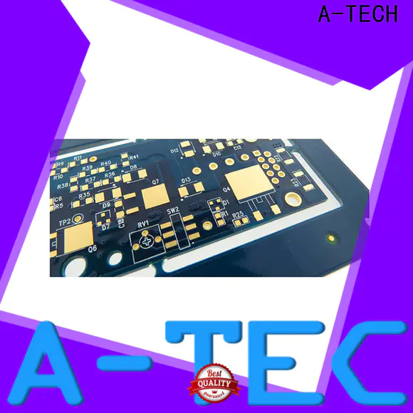

Погружениеное золото или Enig, полное имя - это электрическое никелевое / погружение в погружение, это соотеченность, соответствующая RoHS, которая обеспечивает очень плоскую поверхность и очень надежное припоедение.
Отделка ENIG применяется через осаждение начального слоя никеля на поверхность меди, а затем тонкий защитный слой золота, никельские характеристики твердости, износостойкость, паянию и равномерность осаждения делает эту превосходную поверхность. Тонкий слой золота сохраняет паябильность финиша путем предотвращения окисления высокоактивной поверхности никеля.
В основном толщина золота ENIG составляет 1-5U, а толщина никеля составляет 120-240U ", срок годности погружения погружения Gold PCB может достигать 12 месяцев.
Преимущества погружной золотой отделки
● Отличная плоскостность
● соответствует ROHS
● длительный срок годности
● Подходит для мелкого шага, BGA или меньших компонентов
● провод привязана
● Хорошо для SMD и нажмите Fit
Недостатки погружной золотой отделки
● Дорогой конец
● Черные подушечные проблемы на BGA
A-Tech собственной импульсной золотой линией в доме, это самая использованная отделка на нашем заводе в настоящее время специально для многослойных печатных плат с BGA или тонкой подачей. Мы предлагаем Enig Finish с конкурентоспособной стоимостью и высоким уровнем качества для толщины, так и для внешнего вида.
Общие запросы& Обслуживание клиентов
Тел: 86-755-3318 0782 |. Факс: 86-755-3318 0939
Электронное письмо:Enquiry@atechcircuit.com.
Skype: Atechcircuits.
PCB производство

Штаб-квартира: 1209 ~ 1210 здание Jiayu, Shajiang Rd, город Сонгганг, район Баоань, город Шэньчжэнь, Китай.
Copyright © 2025. A-Tech Circuits Co., Ltd. | Все права защищены
Здравствуйте, пожалуйста, оставьте свое имя и напишите здесь, прежде чем чат онлайн, чтобы мы не пропустим ваше сообщение и не свяжитесь с вами гладко.

