

Связанные продукты


VIA в PAD (VIP) технология относится к VIAS в SMD Pad или BGA Pad из-за небольшого пространства для макета, чтобы избежать потока пайки во внутренний слой или другую сторону в сборке, в основном этот тип через надо надо Быть подключена смолой и пластиной медью, чтобы забросить через него, чтобы сделать его невидимым.
VIA в Pad Technology широко используется в печатных платах высокой плотности, особенно для печатных плат, которые требуют ограниченного пробела BGA и сосредоточены на теплопередаче и высокоскоростной конструкции. Хотя слепые отверстия и похороненные дыры помогают увеличить плотность и экономить пространство на платах, через отверстия по-прежнему лучшее выбору для термических управленческих и высокоскоростных элементов дизайна.
Преимущества через технологии Pad Pad
● Подходит для мелкого поля BGA
● Улучшено тепловое рассеивание
● Предоставляет плоскую поверхность Coplanar для вложения компонентов
● Приводя к более высокой плотности печатных плат и продвижение космического пространства
● Преодолевает высокоскоростные проблемы и ограничения.
● Соответствует близко упакованным требованиям размещения.
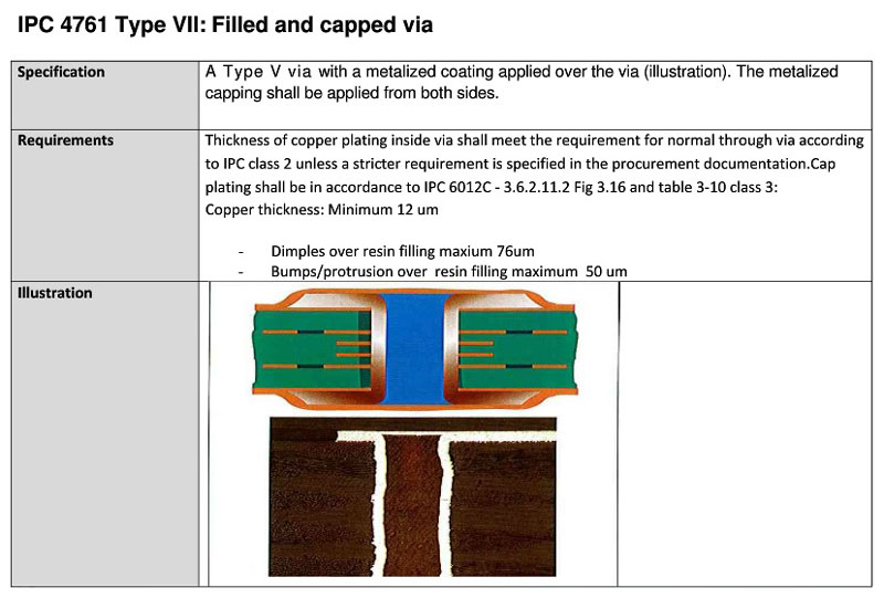
Технология VIA в Pad Cadle определяется в стандарте IPC с IPC-4761 VII
A-Tech произвели много многослойных печатных плат с VIA в конструкции PAD, как в BGA PADS, либо в других полахниках SMD, мы можем полностью подключить VIAS, а затем покрывать медью, чтобы сделать поверхность колодки как квартиру как другие колодки без изменений.
Общие запросы& Обслуживание клиентов
Тел: 86-755-3318 0782 |. Факс: 86-755-3318 0939
Электронное письмо:Enquiry@atechcircuit.com.
Skype: Atechcircuits.
PCB производство

Штаб-квартира: 1209 ~ 1210 здание Jiayu, Shajiang Rd, город Сонгганг, район Баоань, город Шэньчжэнь, Китай.
Copyright © 2025. A-Tech Circuits Co., Ltd. | Все права защищены
Здравствуйте, пожалуйста, оставьте свое имя и напишите здесь, прежде чем чат онлайн, чтобы мы не пропустим ваше сообщение и не свяжитесь с вами гладко.

